The capacitance at the input of the DC-DC converter plays an important role in maintaining converter stability and helps to filter out electromagnetic interference (EMI) at the input. The large capacitance at the output of the DC-DC converter poses a daunting challenge to the power system. Many downstream loads of DC-DC converters require capacitors to operate properly. These loads can be pulsed power amplifiers or other converters that require capacitance at the input. If the capacitance at the load exceeds the limit that the DC power system design can handle, the current in the power system may exceed its maximum rating during startup and normal operation. Capacitors can also cause stability problems in the power system, leading to erroneous system operation and premature power system failure.
In the case of powering large capacitive loads, some simple technical power is maintained in the power system to maintain an efficient and reliable design. Shorten the voltage rise time applied across the load capacitor at startup to keep the current of the power system within its rated range. During normal operation, the charge current flowing into the capacitor can be within the rated range of the power system, and the control loop of the system is adjusted. The circuit maintains the stability of the power system and keeps the voltage of the power system within its rated range.
Start-up considerations
A typical DC-DC converter has a standard rise time when the power system is started, which is determined by the rise time of the internal error amplifier reference. The discharge capacitor placed at the output of the converter will appear as a low impedance load. At this low output impedance, a few switching cycles of the converter can cause a sufficiently high voltage change across the capacitor and force the converter output current to exceed its rating. This capacitor can be pre-charged through the higher impedance path at the converter output. This high impedance component will limit the charging current into the capacitor until the capacitor is charged to a predefined voltage value. Once a predefined voltage value is reached, the high impedance path can be removed or shorted by a low impedance device such as a FET.
The converter can provide maximum current rating through this lower impedance path. When the FET shorts this impedance path, it will allow the converter's full-scale voltage to charge the capacitor. The turn-on time of the FET and the voltage difference between the capacitor and the converter voltage determine the charge current required to charge the capacitor to the full-scale voltage, so setting the predefined voltage value to FET turn-on does not cause the converter to exceed its The point at which the current is rated is very important. The block diagram shown in Figure 1 can be used to charge the capacitor to a preset minimum voltage. U2 is used to control the FET to short-circuit the resistor Z if necessary. The U1 circuit is used with U2 to set the turn-on voltage and load enable.
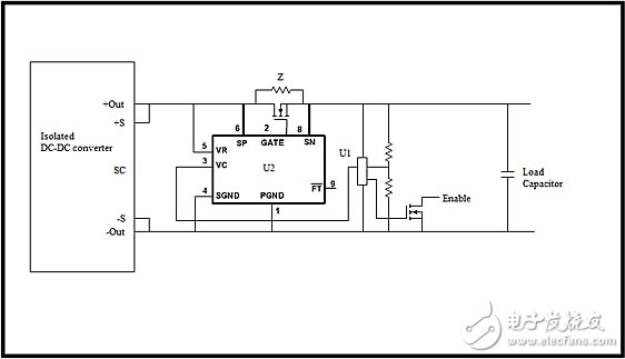
Figure 1: Capacitor pre-charging block diagram
At startup, the converter sees the capacitance as the load and the system load after the capacitor. If the system load needs to draw current from the capacitor during high impedance precharge, the capacitor may not reach the preset charging voltage. Many of the downstream loads of the DC-DC converter have undervoltage lockout capability, which requires very little current in the undervoltage lockout state. If the load does not have an undervoltage lockout function above the preset charge voltage, then an external enable signal should be used. If the load itself is resistive, the voltage to the load can be enabled with a series switch after the capacitor is charged. Figure 2 shows the voltage and current of a system that charges a 10mF capacitor.
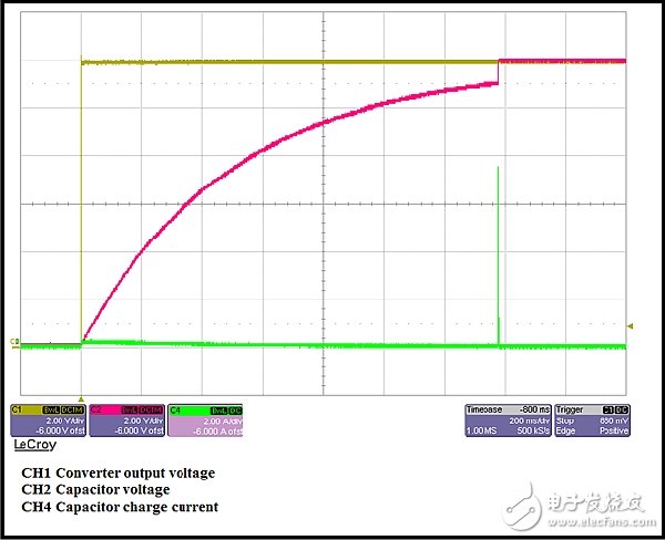
Figure 2: 12V DC Converter for Charging a 10KuF Capacitor
Once the capacitor is charged, the load can begin to draw current from the capacitor and DC-DC converter. Some loads require fast current acquisition. If this requirement exceeds the converter's bandwidth capability, the current will be provided by the capacitor. Once the current is supplied by the capacitor, the voltage across the capacitor drops:
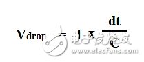
Where Vdrop is the voltage drop across the capacitor, I is the current value required, C is the capacitance value, and dt is the length of the current drawn. The converter will recharge the capacitor to its original value, in which case the converter output current may exceed its rating. The voltage difference between the converter and the fully discharged capacitor divided by the resistance between the two voltages determines the desired recharge current. To reduce system losses, the resistance between the two voltages is usually very low, so the desired recharge current may be higher than the maximum value of the converter. Since the capacitor voltage is close to the setpoint voltage of the converter, exceeding the maximum current value of the converter may mean exceeding the maximum power value of the converter.
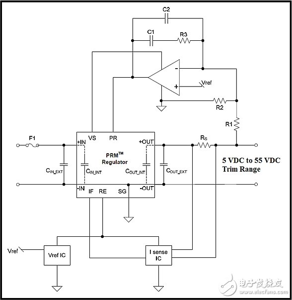
To prevent the converter from exceeding its rated current and rated power during normal operation, the current control block diagram in Figure 3 can be used to control the recharge current after a high di/dt event. This circuit monitors the current on the shunt resistor and limits the recharge current by actively lowering the converter voltage. This limited voltage difference between the converter and the capacitor limits the recharge current of the capacitor, ensuring that the converter is within its current and power limits. As the capacitor voltage rises, the converter voltage also rises until it reaches its set value.
The current limiting method shown in Figure 3 can be used in conjunction with the pre-charging method of Figure 1 to achieve a faster startup process. The precharge circuit charges the capacitor to the minimum regulated voltage of the converter, which then charges the capacitor at full speed at the maximum rated current. Controlling the rate of rise of the output voltage can be achieved for the purpose of controlling the current charged to the capacitor. However, most DC-DC converters have only a narrow control or adjustment range from their nominal set voltage. A typical adjustment interval is ±10%. Some manufacturers can offer a wider range of adjustments, and the converter can even be turned down to -90% of the nominal set voltage. The smaller the voltage adjustment range, the lower the requirements for the enable circuit, as downstream loads typically have an undervoltage lockout function near their minimum operating voltage.
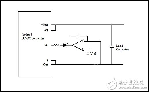
Figure 3: External current limit block diagram
Stability considerations
Once the converter is kept within its limits during startup and operation, then we must ensure the stability of the system. The large capacitance at the output of the DC-DC converter may reduce the phase margin of the system, causing ringing. In order to ensure stable operation of the converter, a minimum of resistance must be used in series with the capacitor. Lead or wire resistance, FET and capacitor equivalent series resistance are all valid components of this resistor. The best way to find the minimum value of this resistor is to use a network analyzer and run the system analysis function to determine the margin of phase and gain. If you don't have a network analyzer, you can also connect a step load to the system to analyze the converter's voltage and current waveforms to ensure that there are no excessive ringing that represents poor stability.
Once the voltage loop has stabilized, the current control loop in Figure 3 can be examined to analyze its effect on system stability. This current control loop is located in the control loop of the DC-DC converter, and its bandwidth should be much smaller than the crossover frequency of the system loop, so the two loops do not interact. In a converter system where the power compensation network is integrated inside the converter, the converter manufacturer can provide enough information to set a suitable crossover frequency for the current control loop. Some converter manufacturers allow designers to optimize the performance of specific applications by adjusting the power control loop.
Figure 4 shows a converter with an external control loop. This control loop can be optimized to provide peak system performance. This external control loop is important in applications where the response time of the power system is critical to proper system operation. This is the case with periodic pulsed load applications where the converter must recharge the capacitor before the next supply pulse. The stability of the system should be verified using a network analyzer or step load test. An unstable system can create a voltage offset that exceeds the rating of the power system components, eventually causing a power system failure.