The Ćuk DC-DC converter designed by Dr. Ćuk is known for its low input and output ripple current and can be used as a buck-boost converter. This design example shows Dr. Ćuk's new converter architecture, a resonant converter that can resonate with large capacitors with very small amounts of inductance, even at relatively low frequencies (eg 50 kHz). Dr. Ćuk tends to keep the switching frequency low, but increasing the frequency can achieve a faster transient response with a smaller LC value.
Many engineers know Slobodan Ćuk (pronounced chook), a designer of the Ćuk DC-DC converter architecture, known for low input and output ripple currents, and as a buck-boost use.
So recently, when I noticed that Dr. Ćuk released a new converter architecture, my interest was immediately tuned.
I have been in touch with this kindly doctor, but I don't know his new design. The prototype seems to have been built, but the details have not been revealed.
This design is considered to be a resonant converter that can resonate with large capacitors with very small amounts of inductance (or even PCB traces) even at relatively low frequencies (eg 50 kHz).
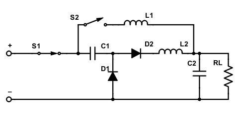
Figure 1: Resonant buck converter and charge pump proposed by Dr. Ćuk.
I found the existing circuit description to be a bit difficult to understand (which undoubtedly shows that my ability is not enough), but here are some of my rough understanding of the design.
If the inductor is ignored (replaced with a short circuit), it is basically a charge pump that operates at a 2:1 ratio.
Imagine that the circuit is more or less balanced. The switch is shown in Figure 1: The input voltage will be divided between C1 and C2. When the switch is flipped, C1 will be in parallel with C2 (via S2 and D1), transferring some power to supplement C2.
By using an inductor, each charge pump (CP) phase is half the resonant period. This reduces current spikes in standard CP designs and allows for duty cycle control of the output voltage without loss of efficiency (because inductance reduces charge transfer rate). I think the control circuit must also take a burst mode to keep the output voltage from rising at low loads because the energy of L2 will be transferred to the capacitor during the charge transfer phase.
D1 and D2 can be actual diodes, if you don't mind the loss, but in most cases it should be a synchronous switch. Dr. Ćuk pointed out that in this case the FET replacing D2 may need to block the current when it is open, just like a diode, but its source replaces the N-channel FET of the D2 cathode (as in a schematic of Dr. Ćuk). The one shown will point a body diode in the wrong direction. Back-to-back FETs may be necessary, but with the correct control circuitry, I think the source may be on the left.
Through this design, I believe that my analytical skills have improved, but if you think that my analysis is wrong, please share your understanding and views on the circuit. Is this a reminder that I need to improve my simulation skills? We will wait and see.
Dr. Ćuk seems to prefer to keep the switching frequency low, but I don't think there is any reason not to increase the frequency so that a smaller LC value can achieve a faster transient response (but this will increase switching losses). What are the specific benefits? Let us look at some examples:
50kHz: 1000μF, 10nH
500kHz: 22μF, 4.6nH 2MHz: 6.8μF, 1nH
Sometimes square root operations are really useful.
So what do you think of the potential value of this design?